Signal Integrity Simulation
Signal Integrity Simulation


WHY Signal Integrity (SI) Simulation?
In low-speed interfaces, signal quality issues are rarely a major concern. However, as transmission speeds continue to increase and chip, package, and passive component designs become more complex, high-speed systems face growing challenges such as reflection, distortion, latency, crosstalk, and impedance mismatch. These issues can significantly impact signal performance and overall system reliability. As a result, signal integrity (SI) has become an essential part of modern product design and development.
WHAT Benefits of Signal Integrity(SI) Simulation?
Driven by the rapid advancement of artificial intelligence (AI), machine learning, 5G, automotive electronics, and the Internet of Things (IoT), electronic product development cycles are becoming increasingly compressed, making time-to-market (TTM) a critical competitive factor. Signal integrity (SI) analysis enables engineers to identify potential high-speed signal challenges early in the design phase and establish optimized layout constraints, minimizing design risks and preventing signal performance issues before prototyping and manufacturing.


WHEN Do You Need Signal Integrity (SI) Analysis?
As high-speed interfaces such as PCIe®, USB, and SATA become increasingly integrated into chips, packages, and printed circuit boards (PCBs), signal integrity (SI) has become a critical consideration in high-speed system design.
iPasslabs | The types of products we can simulate and test
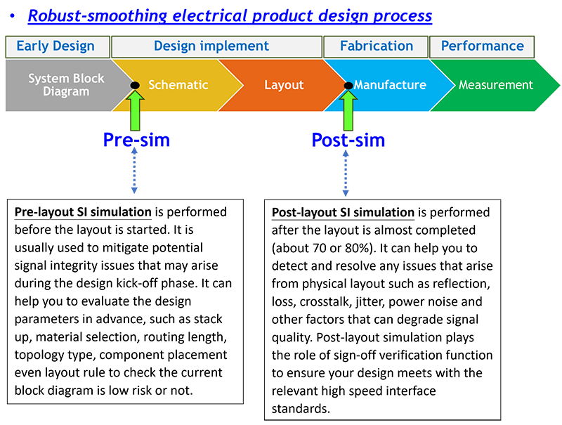
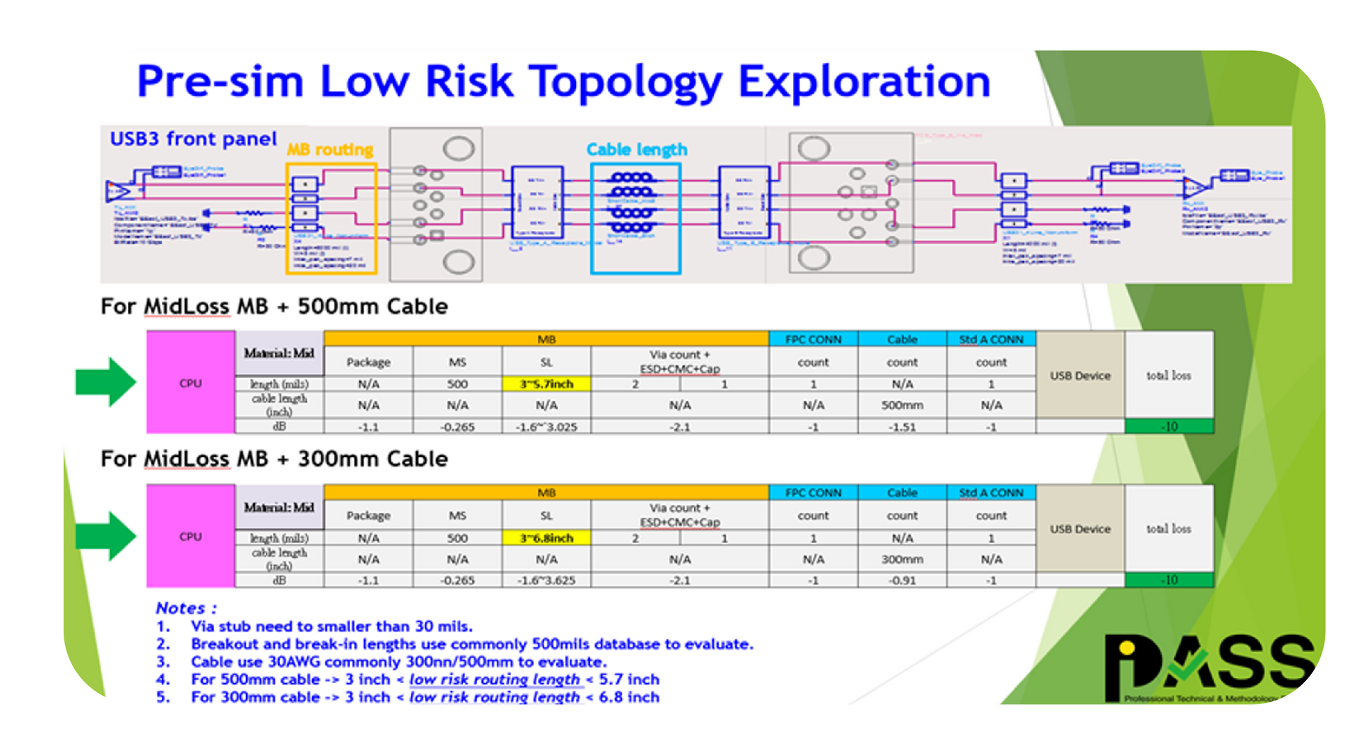
iPasslabs | Signal integrity analysis during the design phase is divided into two types.
iPasslabs | Our Simulation Services and experiences

iPasslabs | Q&A
1.The following data need to be prepared ahead of the simulation project starting:
Stackup:
- Provide information about the PCB stackup, including the number of layers, material types for each layer, and thickness.
Package Model:
- Information about the electrical characteristics of the IC package. This includes details about parasitic components within the package, such as capacitance, inductance, and resistance.
Connector Model:
- If the system includes connectors, please provide the S-parameter models for the connectors. This helps ensure the performance of connectors in high-speed data transmission.
Chip and Device IBIS/IBIS-AMI/DLL Models:
- If IBIS (Input/Output Buffer Information Specification/Non-SerDes), IBIS-AMI (Algorithmic Model Interface/SerDes) models, and DLL (Dynamic Link Library) models are used, it is necessary to provide the corresponding files, that describe the input/output buffer behavior of chips and devices, it enables to provide the most optimized eye diagrams and equalization capability for simulation analysis.
Design Guide:
- Provide any relevant design guides or referenced documents that we can offer best suggestions tailored to the specific simulation project.
2. Can simulation analysis be performed only on the longest trace of the configuration design?
Yes, typically SI simulations adopt the worst-case scenario for evaluation. However, it is suggested to include the shortest trace in the analysis as well because the longest and shortest traces represent the worst cases for loss (IL) and reflection (RL). Analyzing both the longest and shortest traces provides a more comprehensive and accurate signal quality analysis, enhancing production yield.
3.How is simulation analysis executed, and approximately how long does it take for a single run?
Generally, whether it's pre-sim or post-sim analysis, the results will provide suggestions for optimizing the configuration design. Customers can make modifications based on these suggestions, and it can be provided for the second run afterward. Each topology typically takes around 7 weekdays.
4. How is the pricing calculated?
Pricing is determined based on the size of the system (block diagram). For further details, please contact HERE.
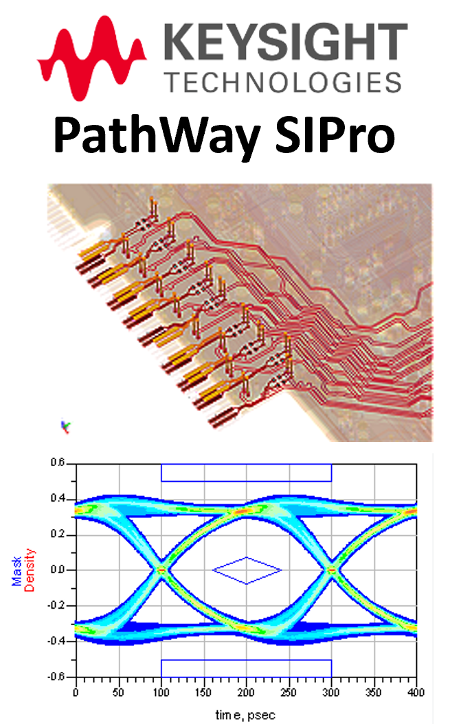
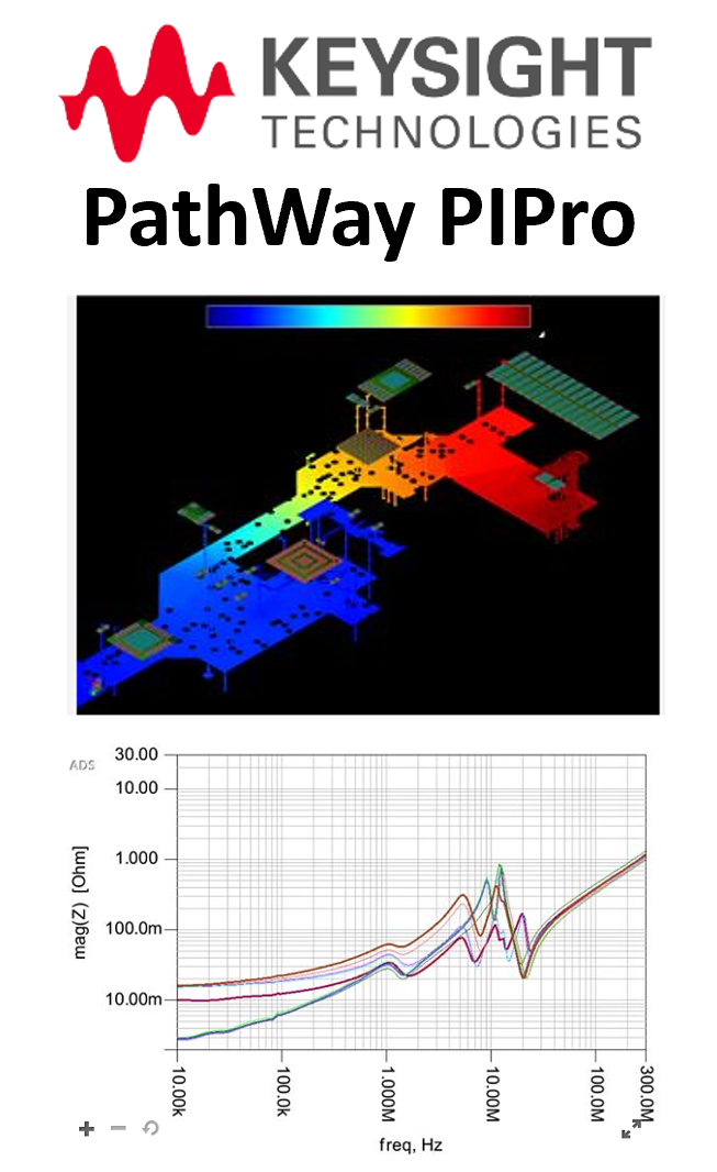
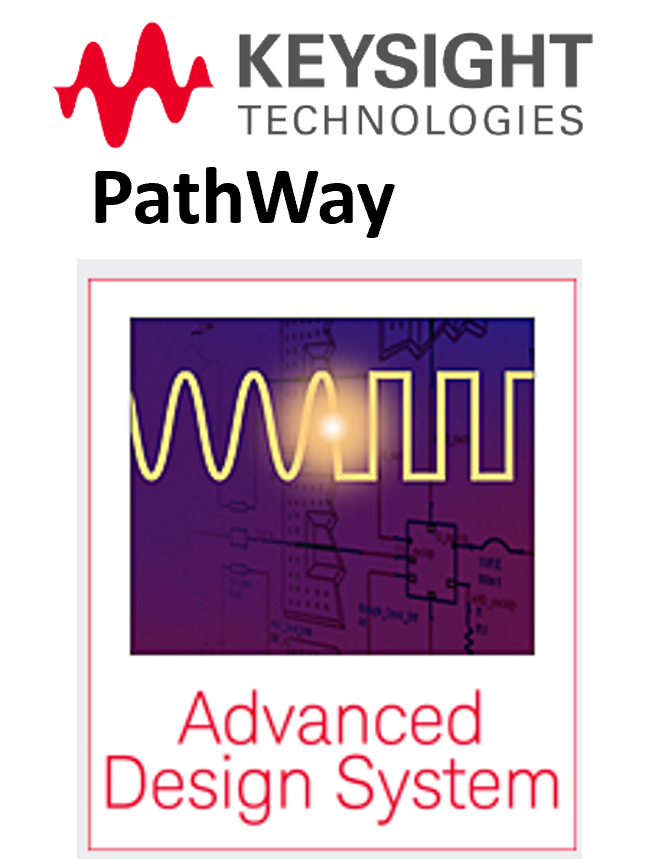
iPasslabs|Simulation Tools