





Why Delta-L Testing Matters More Than Ever in the AI Era?

As AI infrastructure continues to accelerate, competition is no longer driven solely by computing power. Today, success also depends on system integration, product reliability, and time-to-market.
Product performance is no longer determined only by CPUs, GPUs, Switch ASICs, or Retimers. The PCB itself has become an integral part of the high-speed signal channel.
As data rates continue to increase, signal margin becomes increasingly limited. Even minor variations in PCB materials, stack-up, trace routing, impedance control, copper roughness, or manufacturing tolerances can lead to:
- Increased Insertion Loss
- Impedance discontinuities
- Signal reflections
- Differential imbalance
- Reduced Eye Diagram opening
- Higher Bit Error Rate (BER)
- Unstable Link Training
- Compliance Test failures
Therefore, modern high-speed product development requires more than verifying PCB continuity or impedance. It also requires validating the actual transmission performance of the PCB, making Delta-L Testing an essential part of the design validation process.
What is the Delta-L test?
How much signal loss is actually caused by the PCB transmission line itself?
When measuring a PCB channel with a Vector Network Analyzer (VNA), the results include not only the PCB trace, but also the effects of cables, connectors, probes, vias, launches, and test fixtures.
Without removing these influences, the measured data represents the entire measurement system rather than the actual electrical performance of the PCB.
Delta-L Testing utilizes coupons with identical structures but different trace lengths, combined with de-embedding techniques, to remove common fixture and launch effects. This allows engineers to extract the Insertion Loss per unit length and accurately characterize the transmission performance of the PCB itself.
In addition to Insertion Loss, Delta-L Testing can also evaluate:
- Insertion Loss per Unit Length
- Differential Impedance
- S-parameters
- PCB Material Dk/Df Characteristics
As a result, Delta-L has become an important methodology for high-speed PCB characterization, Signal Integrity validation, and PCB material analysis.
What Does Delta-L Testing Validate?
Delta-L is more than measuring a single loss curve. It compares how different design and manufacturing variables affect high-speed signal performance, including:
- Different impedance targets (85Ω / 92Ω / 100Ω)
- Trace width and spacing
- PCB layers
- Trace lengths
- PCB materials
- Temperature conditions (Room Temperature / High Temperature)
Among these, High-Temperature Delta-L Testing has become increasingly important for AI Servers, Switches, NICs, Storage platforms, and other data center applications.
Since data center equipment operates continuously under heavy workloads, elevated temperatures can significantly influence material characteristics and signal transmission.
High-temperature validation helps evaluate:
- Changes in Insertion Loss
- Temperature sensitivity across different PCB layers
- Accuracy of material models
- Correlation between simulation and measured results
- Available Signal Margin under real operating conditions
- Manufacturing consistency among different PCB suppliers
Why do AI products especially need Delta-L Testing?
1. Higher Data Rates Leave Less Signal Margin
As PCIe, Ethernet, and SerDes technologies continue to evolve, even small amounts of insertion loss, reflection, or crosstalk can impact overall system stability.
Simulation alone is no longer sufficient—actual PCB performance must be verified through measurement.
2. PCB Material Specifications Do Not Represent Finished Board Performance
Even when the same laminate material is used, the final electrical performance of a PCB is still affected by stack-up, manufacturing processes, tolerances, copper roughness, and fabrication quality.
Delta-L Testing validates whether the finished PCB performs as originally designed.
3. Identify High-Speed Channel Risks Earlier
By validating PCB coupons before full system integration, engineers can detect design, material, or manufacturing issues early—before System Bring-up, Compliance Testing, or customer qualification.
4. Reduce Board Re-spin Costs and Accelerate Time-to-Market
AI products have increasingly shorter development cycles. A single board re-spin can delay a project by weeks or even months.
Delta-L helps reduce design risks during the early development stage, shorten debugging cycles, improve first-pass success, and accelerate time-to-market.
What are the differences between 20 GHz, 40 GHz, and 65 GHz Delta-L?
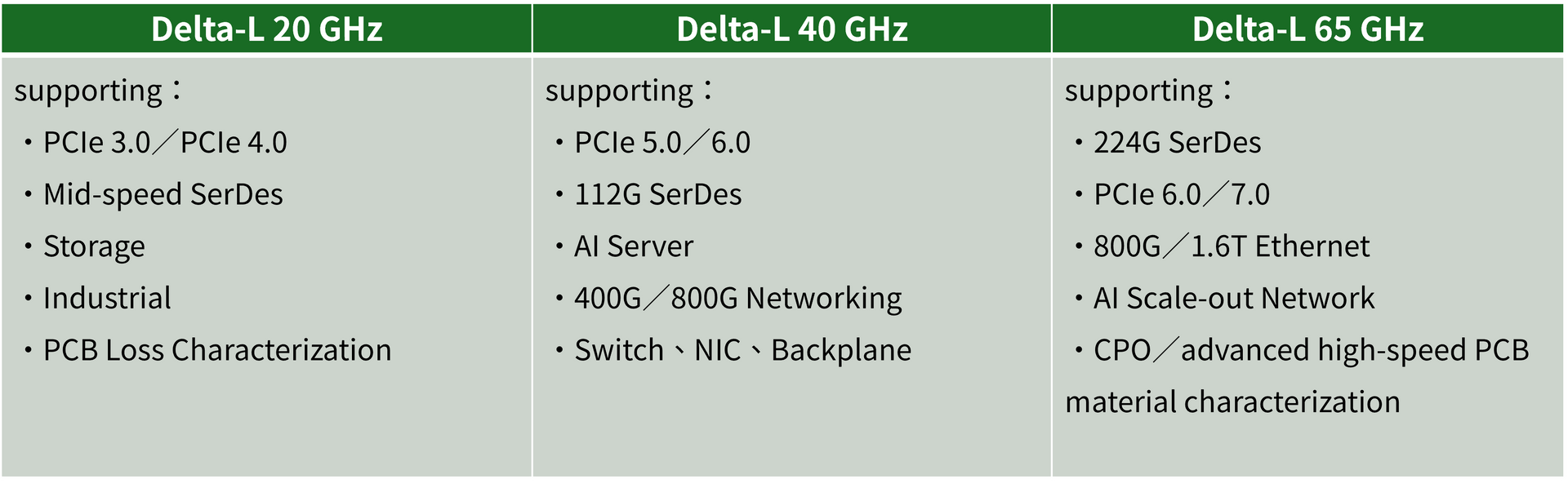
As AI, high-performance computing (HPC), and high-speed networking technologies continue to evolve, PCBs have become far more than circuit boards—they are critical components of the overall high-speed signal channel.
By leveraging Insertion Loss measurements, S-parameter analysis, Differential Impedance characterization, and De-embedding techniques, Delta-L Testing enables engineers to accurately evaluate PCB transmission performance and assess how materials, PCB layers, routing geometry, temperature, and manufacturing processes affect signal integrity.
Its value extends far beyond measurement data by helping engineers:
- Verify PCB Channel Loss Budget
- Improve correlation between simulation and measurement
- Validate PCB materials and manufacturing quality
- Identify high-speed design risks early
- Reduce system debugging and board re-spin costs
- Improve first-pass success
- Shorten product development cycles and accelerate time-to-market
- Establish long-term production quality monitoring
Delta-L Testing is more than a high-speed PCB measurement—it is a critical validation methodology that bridges PCB design, materials, manufacturing, Signal Integrity, System Validation, and overall product success.