





How Silicon Photonics Addresses High-Speed Interconnect Bottlenecks in AI Infrastructure and
the Challenges of Electro-Optical Testing

As Generative AI continues to evolve toward Agentic AI, characterized by autonomous reasoning, planning, and execution, global AI infrastructure is entering a new phase of architectural transformation. From large-scale model training to real-time inference, AI systems require not only greater GPU computing power but also high-bandwidth, low-latency, and energy-efficient interconnect networks to support rapidly growing data exchange demands.
As AI factories scale toward hundreds of thousands or even millions of GPUs, data center performance bottlenecks are extending beyond computing capacity to data transfer efficiency, network bandwidth, and system power consumption. With the adoption of 800G, 1.6T, and next-generation high-speed networking architectures, conventional electrical interconnects face increasingly severe challenges related to signal loss, power consumption, and thermal management. These limitations are accelerating industry adoption of Silicon Photonics (SiPh) and Co-Packaged Optics (CPO).
However, as optical components and high-speed ASICs become integrated through advanced packaging technologies, the challenge is no longer simply achieving higher data rates. It is also ensuring that electro-optical components maintain the manufacturing yield, stability, and reliability required for high-volume production, from wafer fabrication and optical engine integration to final CPO module assembly.
Therefore, establishing a comprehensive electro-optical testing and validation process—from PIC Wafer and Optical Engine Wafer to Singulated Die and CPO Module—is becoming essential to the commercialization and scalable manufacturing of CPO technology.
1. Silicon Photonics: Why Is It a Key Technology for Next-Generation Optical Interconnects?
To understand how CPO addresses high-speed interconnect challenges, it is important to begin with one of its fundamental enabling technologies: Silicon Photonics (SiPh).
Silicon Photonics uses silicon-based semiconductor fabrication processes to integrate optical waveguides, modulators, photodetectors, and other optical components onto a chip. Compared with conventional systems built from discrete optical components, Silicon Photonics enables multiple optical functions to be integrated within a smaller chip footprint through highly integrated Photonic Integrated Circuits (PICs).
The core value of Silicon Photonics extends beyond optical transmission itself. It also lies in its potential to integrate with established semiconductor manufacturing processes and advanced packaging technologies.
From Semiconductor Fabrication to High-Volume Electro-Optical Integration
One of the major advantages of Silicon Photonics is its ability to leverage certain CMOS-compatible processes and existing semiconductor manufacturing infrastructure to support wafer-level fabrication, photolithographic patterning, and high-density component integration.
This allows PIC manufacturing to benefit from the semiconductor industry's extensive experience in process control, wafer inspection, yield management, and high-volume production.
However, CMOS compatibility does not mean that every optical component can be manufactured entirely using standard CMOS processes. For example, light sources typically require III-V semiconductor materials or external lasers, while high-speed photodetectors and specialized modulators may require germanium (Ge), heterogeneous integration, or other material platforms.
The key technical challenge, therefore, is to combine Silicon Photonics, Electronic ICs, and Advanced Packaging into an electro-optical integration platform that is manufacturable, testable, and cost-effective.
Key PIC Components and Their Functions
As the foundation of Silicon Photonics, PICs integrate different optical components to perform optical signal transmission, modulation, reception, and control within a chip.
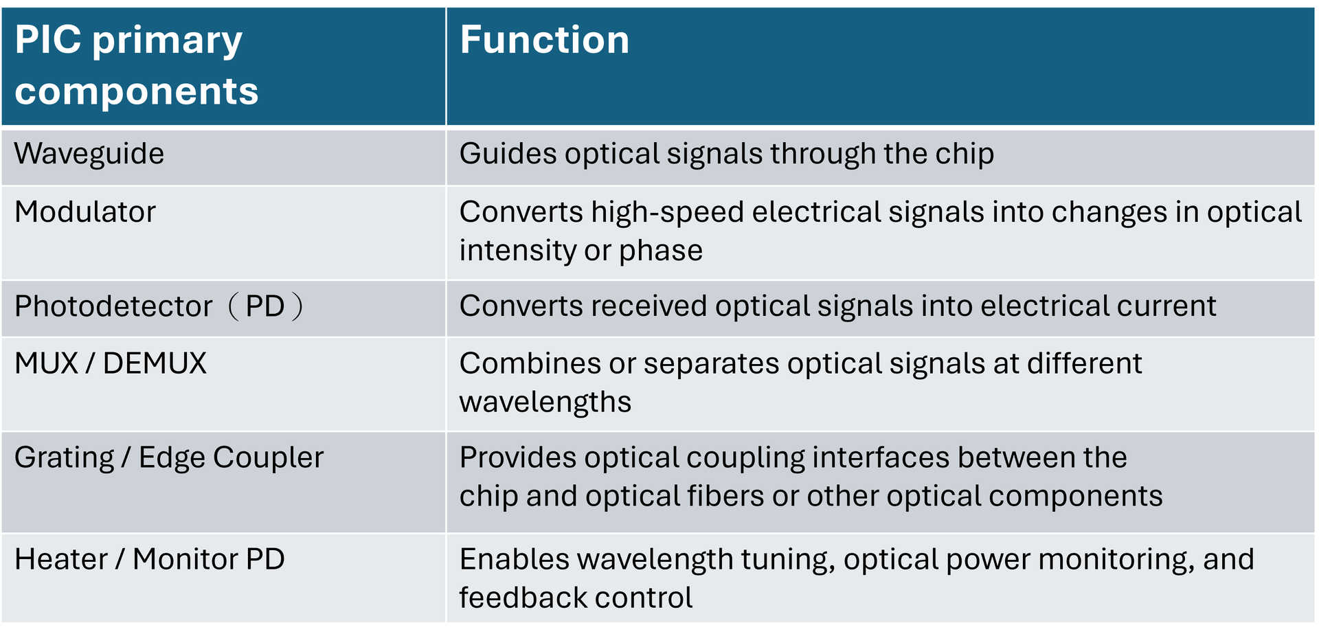
Among these components, modulators play a critical role in high-speed optical communications. Common technologies include the Mach-Zehnder Modulator (MZM) and Micro-Ring Modulator (MRM).
MZMs use optical interference to achieve signal modulation, offering advantages such as high-speed operation and a relatively broad optical operating range. MRMs, on the other hand, rely on micro-ring resonance and enable high-density, low-capacitance device designs, although they are more sensitive to wavelength and temperature variations.
Different modulator technologies involve trade-offs in bandwidth, power consumption, footprint, linearity, and thermal stability. As a result, no single modulator architecture is suitable for every high-speed optical interconnect application.
Although PICs can integrate multiple optical functions onto a chip, electronic circuits are still required to drive, receive, and control signals when communicating with high-speed ASICs. This introduces another essential component of electro-optical integration: the Optical Engine.

2. From PIC to Optical Engine: The Core Electro-Optical Integration Architecture of CPO
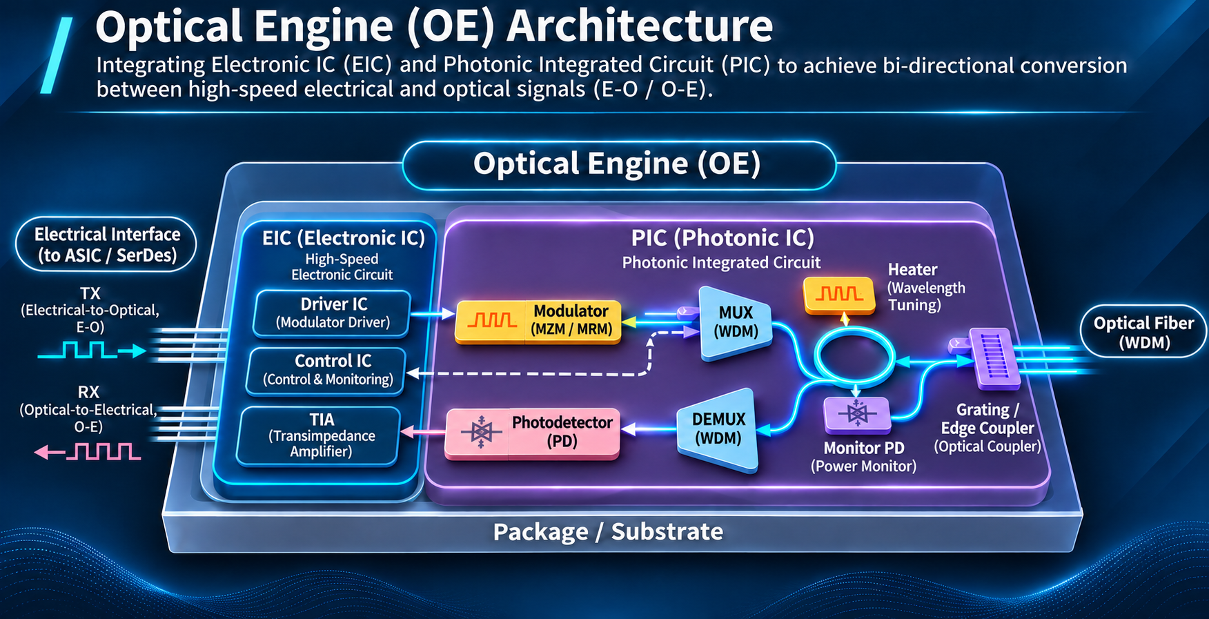
When a PIC is integrated with an Electronic Integrated Circuit (EIC), the resulting assembly can form an Optical Engine capable of electrical-optical signal conversion.
The PIC primarily handles optical signal generation, modulation, transmission, wavelength multiplexing and demultiplexing, and detection. The EIC is responsible for driving, receiving, amplifying, and controlling high-speed electrical signals.
A typical Optical Engine may include Driver ICs, Transimpedance Amplifiers (TIAs), Control ICs, and other signal-processing circuits, depending on the system architecture.
How Does an Optical Engine Perform E-O / O-E Conversion?
On the transmit (TX) side, high-speed electrical signals from the ASIC are amplified by a driver and used to drive optical modulators on the PIC. The data is encoded onto an optical carrier and then transmitted through optical fiber.
On the receive (RX) side, incoming optical signals are converted into electrical current by a photodetector. The resulting signal is amplified by a TIA and processed by subsequent receiver circuitry before being delivered to the ASIC.
It is important to note that the laser source in a CPO Optical Engine may be implemented using an External Laser Source (ELS) or another integration approach. Not all Optical Engines integrate the laser directly onto the PIC.
Through the integration of PICs and EICs, Optical Engines serve as a critical bridge between high-speed electronic systems and optical fiber networks.
However, an Optical Engine is not equivalent to CPO itself. The architectural significance of CPO lies in further shortening the high-speed electrical transmission path between the Optical Engine and the ASIC.
3. CPO: Bringing Optical Engines Closer to the ASIC
The fundamental concept of Co-Packaged Optics (CPO) is to integrate Optical Engines and high-bandwidth ASICs within a shared package or advanced packaging platform.
In conventional pluggable optics architectures, high-speed electrical signals from a switch ASIC typically travel through the package, PCB traces, and connectors before reaching front-panel optical transceivers.
CPO moves Optical Engines much closer to the ASIC, significantly shortening the high-speed electrical path while using optical fibers for subsequent data transmission.
This architecture can reduce certain high-speed electrical channel losses, decrease reliance on long-reach electrical signal compensation, and improve bandwidth density and overall system energy efficiency.
Engineering Challenges Introduced by High-Density Integration
However, the advantages of CPO come with additional engineering complexity.
When Optical Engines and high-power ASICs are integrated within the same packaging environment, thermal management, optical fiber coupling, packaging stress, component serviceability, and long-term reliability become more challenging.
Furthermore, CPO will not immediately or completely replace conventional pluggable optical transceivers. Different optical interconnect solutions are expected to coexist, depending on bandwidth requirements, transmission distance, cost, maintenance considerations, and deployment scenarios.
In other words, while CPO addresses certain interconnect limitations by shortening high-speed electrical paths, it also concentrates design challenges that were previously distributed across separate components and modules into a more highly integrated packaging environment.
Therefore, the next critical challenge for CPO is no longer simply achieving high-speed electro-optical conversion, but ensuring component performance, manufacturing yield, and system reliability after integration.

4. Technical Challenges of Highly Integrated CPO: From Component Performance to System Reliability
CPO brings semiconductor manufacturing, optical components, high-speed electronic circuits, and advanced packaging together on a single technology platform. By shortening the high-speed electrical path between the Optical Engine and the ASIC, CPO has the potential to reduce signal transmission loss, improve energy efficiency, and increase bandwidth density. However, as electro-optical integration becomes more advanced, design challenges that were previously distributed across separate components and modules are increasingly concentrated within a more complex packaging environment.
The engineering challenge of CPO is not simply whether individual components meet their performance requirements, but whether optical, electrical, and packaging structures can maintain stable signal quality and long-term reliability after integration.
At the optical component level, the Optical Insertion Loss of a PIC directly affects the Optical Power Budget of the link, while the Extinction Ratio and Bandwidth of a modulator determine the quality of high-speed optical modulation. If component performance falls below design requirements, it may cause distortion in high-speed PAM4 signals and ultimately degrade overall transmission performance.
At the electro-optical conversion level, the integration quality between the Electronic IC (EIC) and PIC is equally important. For example, bandwidth matching between the Driver and Modulator affects transmit signal quality, while the receiving performance of the Photodetector and Transimpedance Amplifier (TIA) determines receiver sensitivity and signal recovery capability. Therefore, Optical Engine validation cannot focus solely on individual optical or electrical components. It must also verify the integrated E-O (Electrical-to-Optical) and O-E (Optical-to-Electrical) conversion performance.
When the Optical Engine is further co-packaged with a high-speed ASIC, the system must address increasingly complex thermal management and mechanical reliability challenges. Heat generated by a high-power ASIC may affect the operating conditions of nearby optical components. Mechanical stress during packaging, differences in material thermal expansion, and optical fiber coupling misalignment may also introduce additional optical loss or temperature-dependent performance drift.
In addition, high-speed electrical interfaces still require careful consideration of Signal Integrity (SI), Power Integrity (PI), and system-level signal transmission quality. Even though CPO shortens high-speed electrical paths, electrical interconnects within the package, power supply stability, and interactions between electro-optical components remain critical considerations in overall system design and validation. These challenges demonstrate that CPO reliability is not simply the sum of individual component performance. Instead, it depends on the integration quality among the PIC, EIC, Optical Engine, advanced packaging, and high-speed ASIC.
More importantly, if optical or electrical failures are discovered only after a highly integrated Optical Engine has been packaged with a high-value ASIC, the resulting rework costs, packaging losses, and impact on overall manufacturing yield can be significant.
Therefore, the key to transitioning CPO from technology development to high-volume manufacturing is not only improving component performance, but also identifying potential defects early and preventing defective components from entering subsequent high-cost integration and packaging processes.
This makes testing and validation strategies an essential part of CPO manufacturing technology.
5. From Technology Validation to High-Volume Manufacturing: Why Does CPO Require a Staged Testing Strategy?
As Silicon Photonics and Co-Packaged Optics are gradually adopted in AI data centers, electro-optical integration is progressing from research and development toward real-world product deployment.
In 2026, NVIDIA announced mass-production progress for its Spectrum-X Ethernet Photonics platform, indicating that CPO is beginning to enter commercial applications in high-end AI networking switches. Its technology design places particular emphasis on detachable fiber connections, pre-tested Optical Engines, and automated assembly, highlighting the growing importance of manufacturing yield and serviceability.
Compared with conventional electronic ICs, CPO manufacturing involves a broader range of cross-disciplinary integration processes, including PICs, EICs, Optical Engines, optical fiber coupling, advanced packaging, and high-speed ASICs.
Because different types of defects may arise during component fabrication, integration, and packaging, relying solely on final CPO Module testing can make it difficult to identify the source of failures at an early stage. It may also increase subsequent rework and scrap costs.
Therefore, CPO manufacturing requires a Test Insertion Strategy, in which appropriate testing checkpoints are established at different manufacturing and integration stages. This enables progressive verification of component performance and integration quality, rather than concentrating all validation activities at the final module stage.
This approach of moving testing earlier in the manufacturing process is also known as Shift-Left Testing. Its primary objective is to identify components that fail to meet specifications before they enter high-cost packaging processes, thereby reducing downstream integration risks and improving overall manufacturing efficiency and yield management.
From PIC Wafer and Optical Engine Wafer to Singulated Die and the final CPO Module, each manufacturing stage has its own testing priorities. Through staged validation, manufacturers can progressively verify the performance of optical components, electro-optical conversion circuits, and integrated systems, establishing a quality foundation for subsequent packaging and high-volume production.
The competitive focus of CPO technology is expanding beyond electro-optical integration capabilities to encompass comprehensive testing, validation, and manufacturing yield management.
This raises another important question: What optical, electrical, and system-level characteristics must be validated at each stage of CPO manufacturing and integration? And how can testing strategies help reduce packaging risks and improve overall manufacturing yield?
In the next article, we will explore the four-stage CPO testing architecture—from PIC Wafer and Optical Engine Wafer to OE Singulated Die and CPO Module—along with the key validation parameters and technical challenges at each stage.